scia Systems was founded 2013 and is located in Chemnitz, Germany. The company manufactures advanced ion beam and plasma processing equipment for the production of microelectronics, MEMS and precision optical components, in both high volume production as well as R&D applications. scia Systems provides highly reliable tools together with outstanding technology support. The systems accommodate all standard wafer sizes and may be customized to handle samples in a wide range of sizes. The tools are flexible and modular in design, allowing several vacuum process chambers to be combined into cluster or in-line solutions, according to customer-specific requirements.
Ion Beam Etching (IBE) / Milling (IBM):
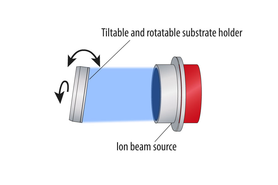
Our IBE tools generate plasma with MW or RF sources. The positive ions are extracted through a 3-grid system to form a broad ion beam which physically bombards (etches) material from the substrate surface. Any material with a sufficiently high melting temperature can be etched with IBE.
The wafer substrate can also be rotated for high uniformity, or tilted to change incident angle. SIMS or OES end point detection is an option to enhance process monitoring.
Equipment Offered:
Ion Beam Trimming (IBT) / Figuring (IBF):
For IBT (Trim 200) and IBF (Finish 1500), positive ions within a RF plasma source is extracted through a 3-grid system and focused to small spot size ~10mm, which scans across the substrate while varying dwell time to adjust the amount of locally etched material.
This can be applied for applications such as thin film thickness uniformity improvements or post CMP correction down to 0.5nm RMS, as well as adjusting the surface form error of curved optical substrates.
Equipment Offered:
Magnetron Sputtering:

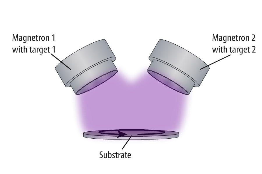
In magnetron sputtering, there is a dense plasma confined at the cathode surface by a permanent magnetic field. Positive ions are accelerated towards the cathode target and physically bombard target material off towards the substrate.
There is a single magnetron configuration (Magna 200) which deposits one target material across the entire surface of the wafer. The target can be a single element or compound, or have a metal target combined with reactive gasses such as oxygen or nitrogen to deposit dielectrics.
The co-sputtering configuration (Magna 200) contains up to 4 smaller magnetron targets. Different target materials can be combined to sputter alloys, or same target materials can be combined for bipolar sputtering. There is also reactive sputtering capabilities in this configuration.
The dynamic deposition configurations (Multi 300 / 680 / 1500) the substrate moves in a linear or orbital path across rectangular magnetron targets for precise multilayer coatings. This configuration is mainly used for depositing on large substrates, up to 1.5m.
In all magnetron sputtering tools, the substrate is capable of rotating to improve uniformity.
Equipment Offered:
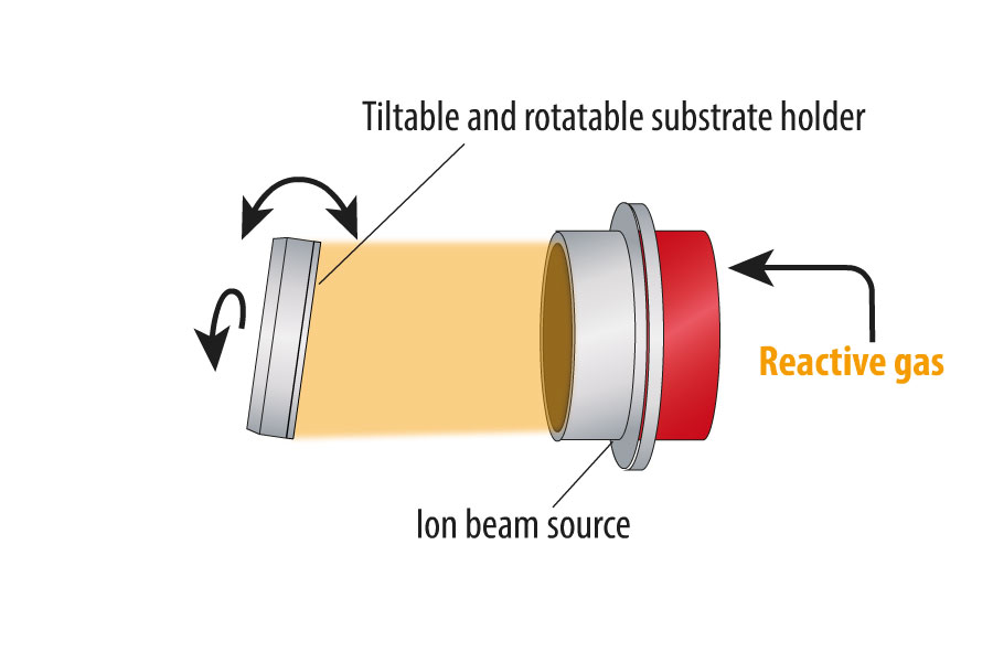
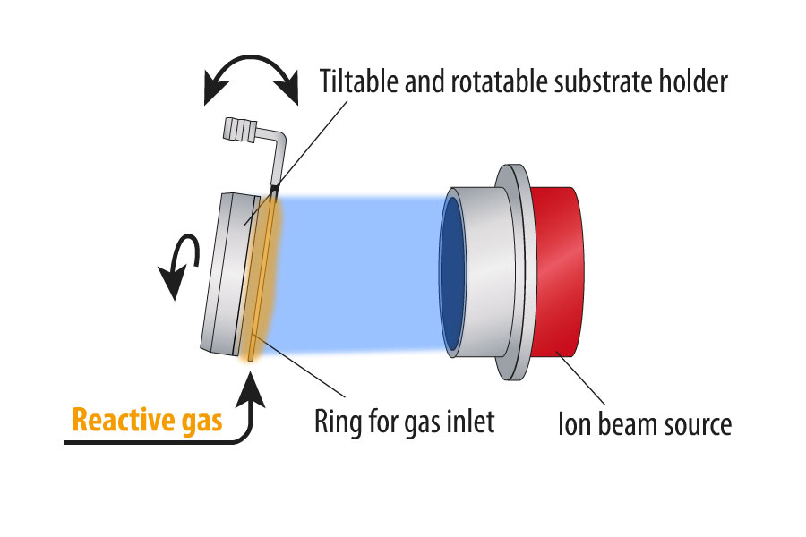
Ion Beam Sputtering (IBS):
In IBS, a RF source is used to generate a plasma then a grid system extracts and accelerates a broad ion beam towards the target material drum. These ions physically bombard target material which is deposited onto the substrate surface. As with magnetron sputtering, reactive gasses can be introduced to deposit dielectric materials.
Low chamber pressure and process temperatures allows for dense thin film depositions with outstanding refractive index and low absorption losses. The rotatable target drum allows for in-situ target switches. An optional second ion beam source can be equipped for surface pre-clean and/or deposition assist (dual ion beam sputtering – DIBS).
Equipment Offered:
PECVD or RIE:
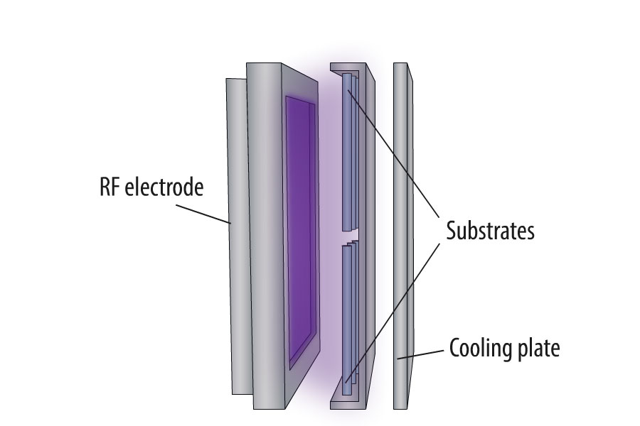
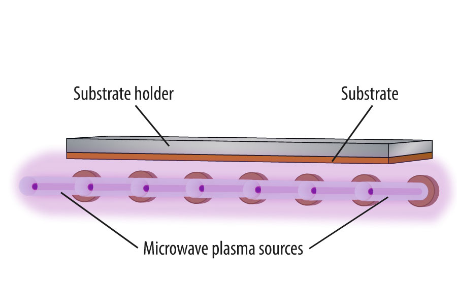
For plasma enhanced chemical vapor deposition (PECVD), precursor gases are vaporized by plasma excitation, which then condense onto the substrate surface. In reactive ion etching (RIE), reactive gases are ionized by plasma excitation, then physically and chemically etch the substrate surface. High reactivity in RIE allows for parameter tuning to control selectivity, trench profiles, and etch rates. The plasma excitation occurs from a RF electrode (Batch 350) or microwave antenna setup (Cube 300 / 750).
Equipment Offered:
Electron Beam (E-beam) Evaporation:
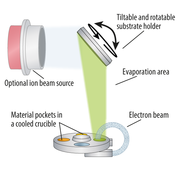
For e-beam evaporation, current through a tungsten filament results in electron emission, which is then accelerated into a e-beam by high voltage. This e-beam is directed and focused into the crucible by a magnetic field. The material is energized to create an evaporation flux onto the substrate.
The substrate is rotatable to improve uniformity. It is also tiltable to allow for glancing angle depositions (GLAD). An optional second ion beam source can be equipped for surface pre-clean and/or deposition assist.
Equipment Offered:
Dry-cleaning:

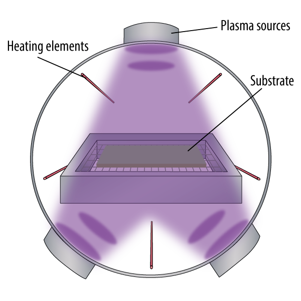
The dry cleaning systems is capable of removing substrate surface contaminations for sensitive applications. Conducted at very low chamber pressures using ultra high vacuum, contaminates can be removes by vacuum desorption, thermal desorption and plasma treatment.
Equipment Offered: