Ion Beam Trimming – Uniformity Improvement:
Thickness uniformity is an important spec for many PIC applications. Ion beam trimming is a proven technology enabling volume manufacturing of highly uniform films.
The process is based on a physical sputter etch, and thus has been proven on almost all applicable materials. Please reach out to discuss your specific application or material!
The example below gives an example for trimming SiNx films.
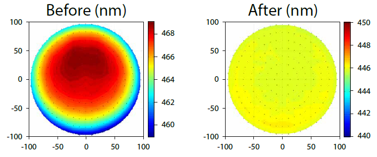
| Before | After | |
|---|---|---|
| Thickness Mean (nm) | 465 | 446 |
| Thickness Range (nm) | 14 | 1 |
| Thickness Uniformity | 3.0% | 0.2% |
| Roughness, Rq (nm) | 0.41 | 0.22 |
| Processing Time | <5min per 200mm wafer | |
Ion Beam Milling or Etching – Waveguides:
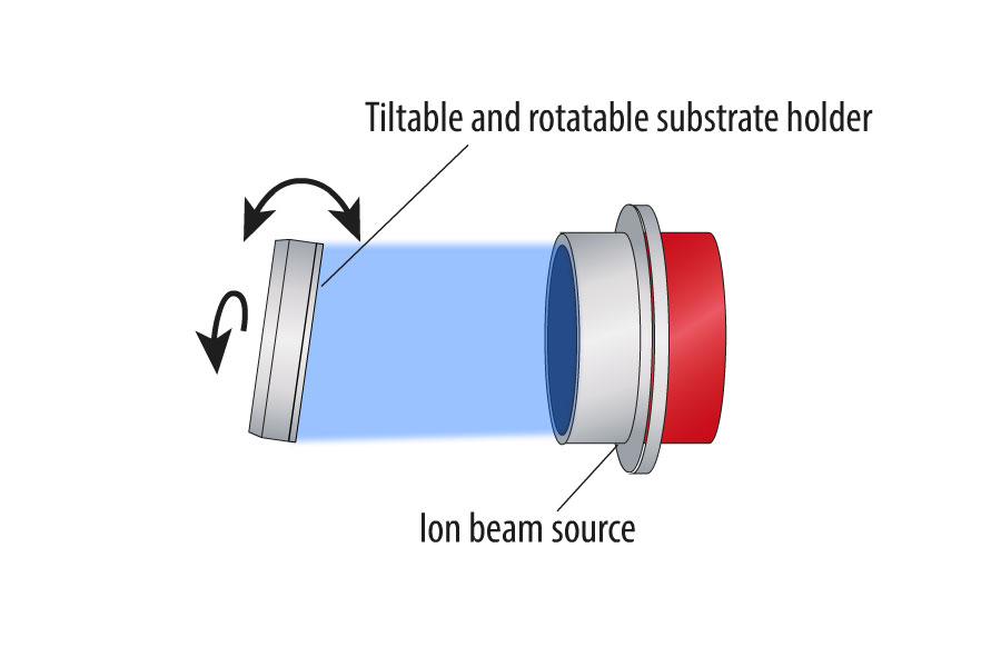
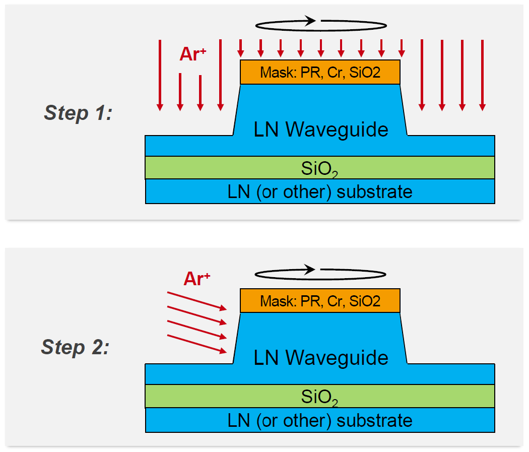
Waveguides for PIC applications require vertical and smooth sidewalls to satisfy optoelectronic properties. Certain waveguide materials, such as lithium niobate (LN, LiNbO3) and others, are difficult to etch and reach these specs with common ICP-RIE technologies. Ion beam etching (IBE) has been used for these materials in R/D and manufacturing to achieve the best optical devices.
Since IBE is a physical etching method, it is capable of etching all materials. F and Cl -based reactive gases can be supplemented to tune etch selectivities.
- Directionality of etch
- Vertical, smooth sidewalls
- Slanted, smooth sidewalls
- Excellent uniformity <1%
- In-situ sidewall redeposition/fencing removal
- SIMS or OES end point detection and etch material monitoring
- Tiltable and rotatable substrate
- He backside contact cooling with water
- Chiller available for even lower temperatures
- Capable of adding F- & Cl- gasses to Ar mixture for reactive ion beam etching