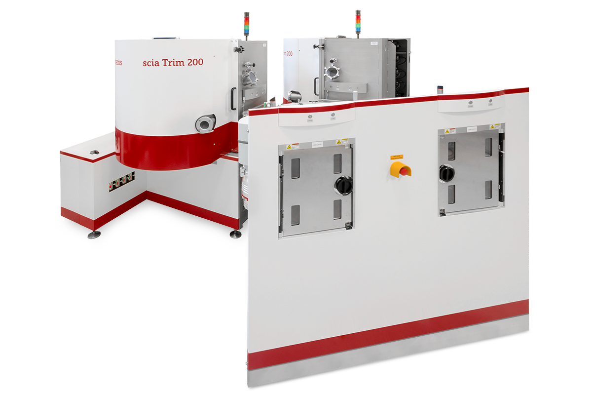
The scia Trim 200 is designed for high precision film thickness trimming of substrates up to 200mm without being constrained by film and wafer material limitations.
The scia Trim 300 for substrates up to 300mm is also available, but specs not listed below. Please contact us for more information.
The scia Trim 200/300 is suitable in a research setting, as it is very versatile ion beam etching tool with a small, scanning spot size. The tool is also optimized and well-tested for many customers in a high volume manufacturing environment for yield improvement, among other applications, and accommodates a standard semiconductor cassette handling robot. Single chamber or cluster tools with two process chambers and two cassette load-locks are available.
Principle:
- Focused broad ion beam scans across wafer surface
- Amount of local material removal is controlled by adjusting the dwell time
- Vertical setup allows for low contamination
Features and Benefits:
- Yield improvement
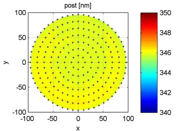
- Ability to tune atomic level (0.1nm) film thickness homogeneity
- Sub-nanometer min-removal point with zero base etch (ZBE) function
- Etch unconstrained by wafer and film material
- Throughput and maintenance optimized for low production costs
- Helium backside cooling with water
- Allows for processing with photoresist with adequate wafer cooling
- Option for electrostatic chuck (ESC) to eliminate edge exclusion zone

Applications:
- Frequency trimming of bulk acoustic wave (BAW) or surface acoustic wave (SAW) filters
- Thickness trimming of silicon on insulator (SOI), quartz, lithium tantalate (LT) or lithium niobate (LN) wafers
- Film thickness error or step height correction in thin film head (TFH) manufacturing
- Dimensional correction in manufacturing of MEMS components
- Form error correction for X-ray mirrors
Technical Specifications:
| SPECIFICATION | DESCRIPTION |
|---|---|
| Substrate size | up to 200mm |
| Substrate holder | Water-cooled, helium backside cooling contact |
| Axes motor | Maximum velocity 0.5 m/s Maximum acceleration 15 m/s² |
| Ion beam source | 37 mm circular RF source (RF37-i) with 7-15mm (FWHM) 80mm circular RF source (RF80-i) with 12-20mm (FWHM) |
| Neutralizer | Hot filament neutralizer (N-Fil) DC plasma bridge neutralizer (N-DC) RF plasma bridge neutralizer (N-RF) |
| Typical removal rate | SiO2: RF37-i ~ 6 x 10⁻³ mm3/s RF80-i ~ 11 x 10-3 mm3/s |
| Film variation after trimming | < 0.5 nm RMS (dependent on input quality) |
| Wafer throughput | 15 Wafers/hr (50nm Si on 150mm wafer) |
| Base pressure | < 1 x 10⁻⁶ mbar |
| System dimension (W x D x H) | 2.80 m x 1.40 m x 2.20 m Single chamber with cassette handler (without electrical rack and pumps) |
| Configurations | Single chamber with single substrate lock lock or cassette handler Cluster system with 2 process chambers and cassette handling |
| Software interfaces | SECS II / GEM, OPC |