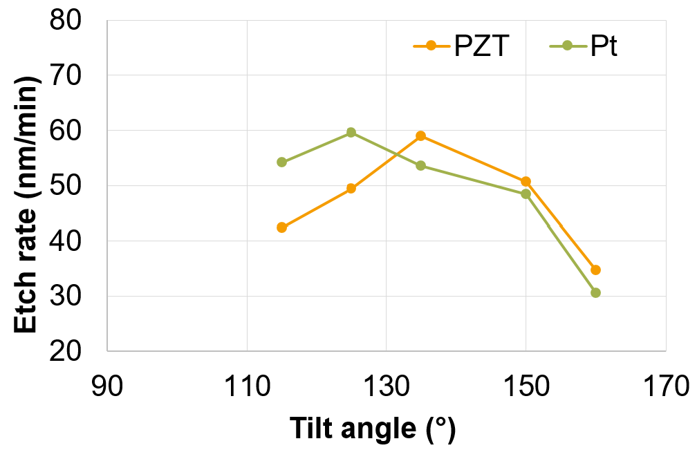
IBE can be used for etching of piezoelectric materials like PZT, AlN, and AlScN. One of the issues when ICP-RIE dry etching such materials is sidewall redeposition/fencing. With IBE, a 2 step process can be used to 1) etch at an vertical ion incident angle to desired depth, then 2) etch at a shallower angle to remove any sidewall redeposition or fencing that occurred during the first etch step. Changing the ion incidence angle can also allow for selectivity tuning, as shown in the figure below.
Since IBE is an inert, physical sputter etch, it can also etch Cu, Pt, or other noble metal electrodes that are often found in such piezoelectric device stacks. The metal electrode(s) can be etched in the same piezo etch run, effectively eliminating the need for additional lithography and or metal liftoff steps. scia Mill systems are also designed with a water cooled chuck and helium backside cooling contact to the wafer. Proper wafer cooling enables the use of PR without observing reflow or damage during the etch process.
Principle of IBE:
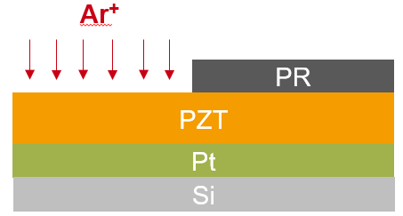
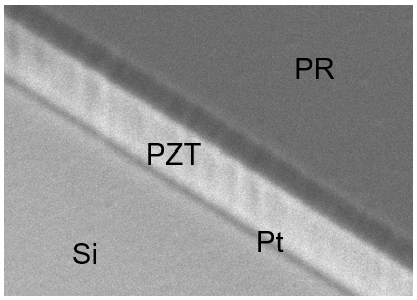
Application Example:
IBE of PZT and Pt with photoresist mask.
Process Example:
Etch rates as a function of ion incident angle.