Some applications require ultra high wafer or thin film total thickness variation (TTV) or planarization that is unachievable with typical processes such as chemical-mechanical polishing (CMP). In such cases after CMP, the scia Trim 200 and 300 can be used to reach the desired thin film uniformity or wafer planarization. The scia Trim tools have a focused argon ion beam that scans across the wafer surface while varying the dwell time to physically etch material off the surface. This physical etching method works for all wafer materials. The tool and process are optimized for high volume production of wafers to provide significant yield improvement.
- SOI
- LN on Si
- LT on Si
- SiC
- Quartz
- and more…
SiC Wafers:
- Successful studies on planarization
- Shape forming and Surface Smoothing processes
- Please contact us for SiC trimming experimental data
- Average removal up to 8um with processing times ranging from 10mins-1hr / per wafer
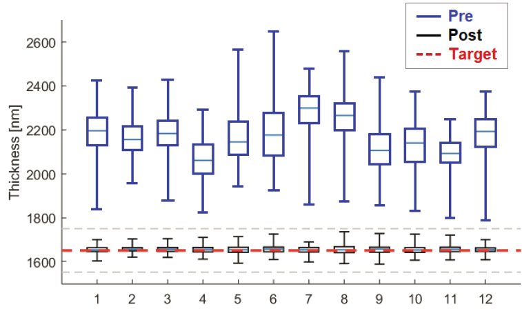
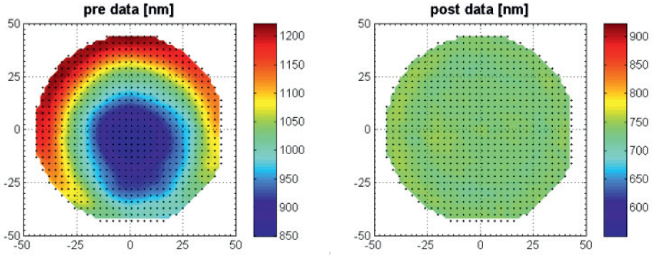
Si Trimming on SOI Wafers:
- 200mm wafers
- Post CMP trimming process
- Average removal ~500nm
- Processing time ~15mins
- Would vary depending on wafer size and desired final thickness variation
- Roughness unchanged
| Before | After | |
| Thickness Variation (nm) | ± 900 | ± 100 |
Lithium Tantalate (LT) on Silicon Wafer:
- 200mm wafers
- Post CMP trimming process
- Average removal ~300nm
- Roughness unchanged
| Before | After | |
| Average Thickness (nm) | 1036 | 736 |
| Thickness Variation (nm) | ± 101 | ± 6 |
scia Trim 200 / 300:
- Designed for high precision film thickness trimming
- Can reach angstrom level accuracy
- Handles substrates up to 200mm and 300mm, respectively
- Can process smaller substrate sizes with quick conversion
- Optimized for high volume manufacturing (HVM)
- World leader >150 chambers world wide
- MEMS, SC, optics, astronomy
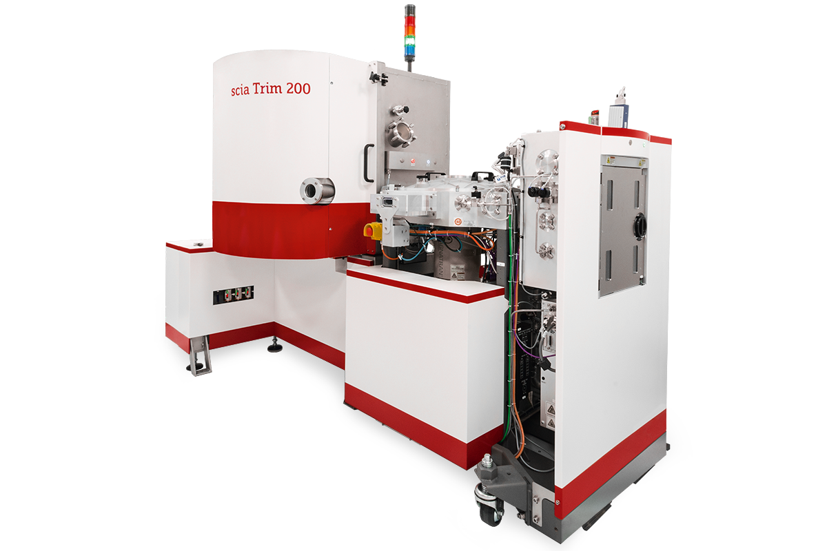
Can also be configured in 2 system 2 cassette cluster,
or single wafer loader.