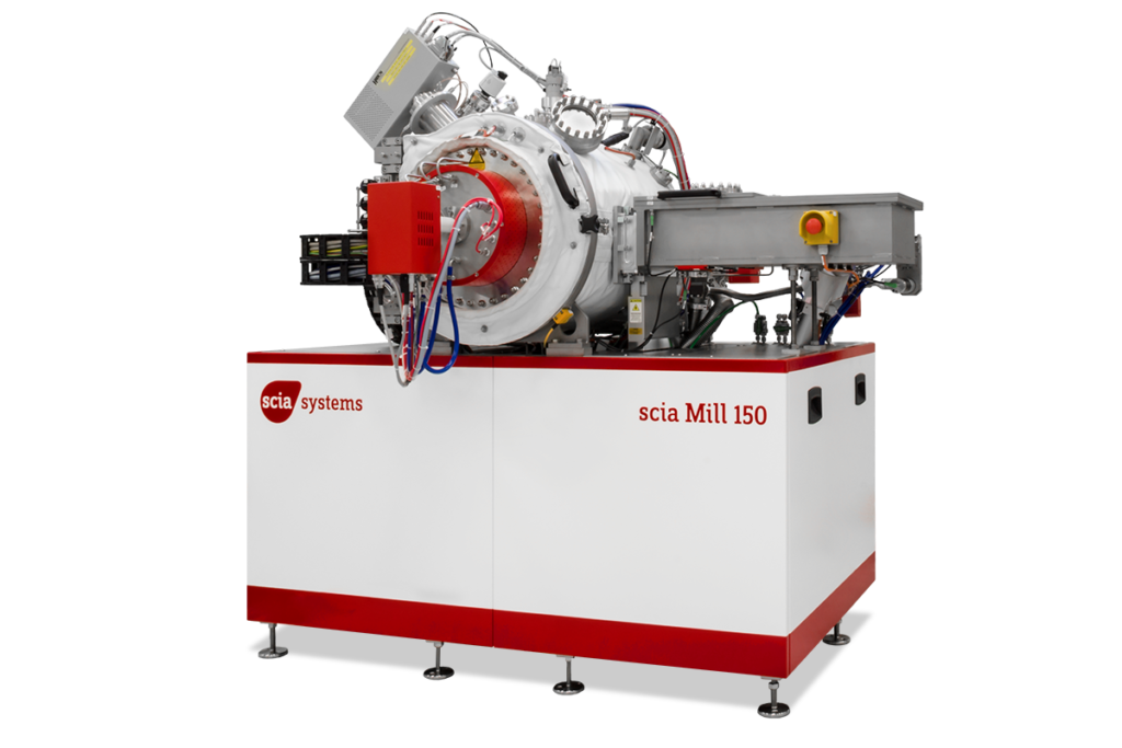
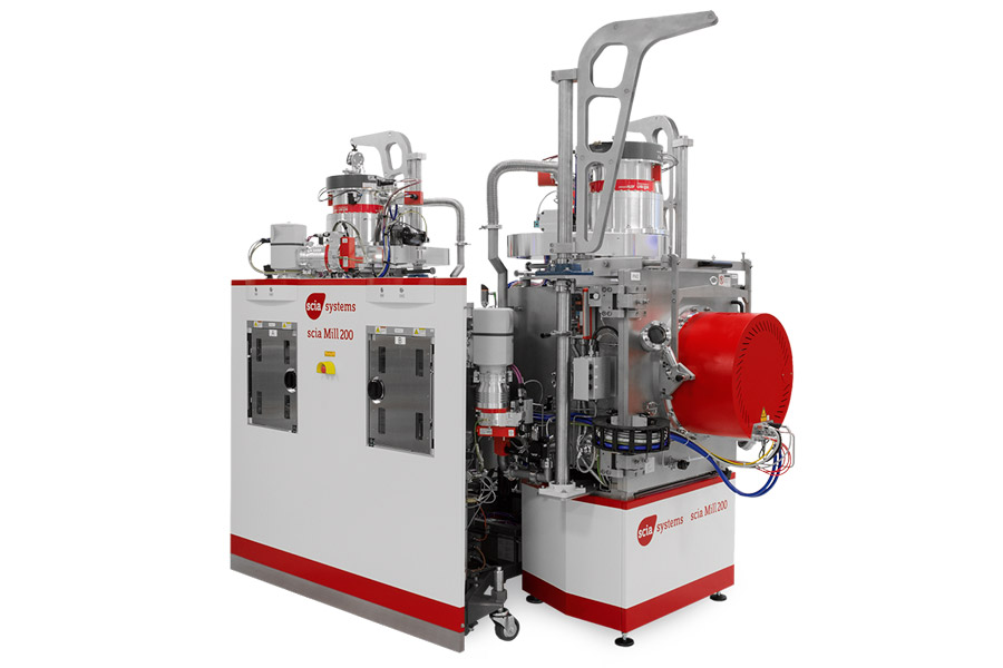
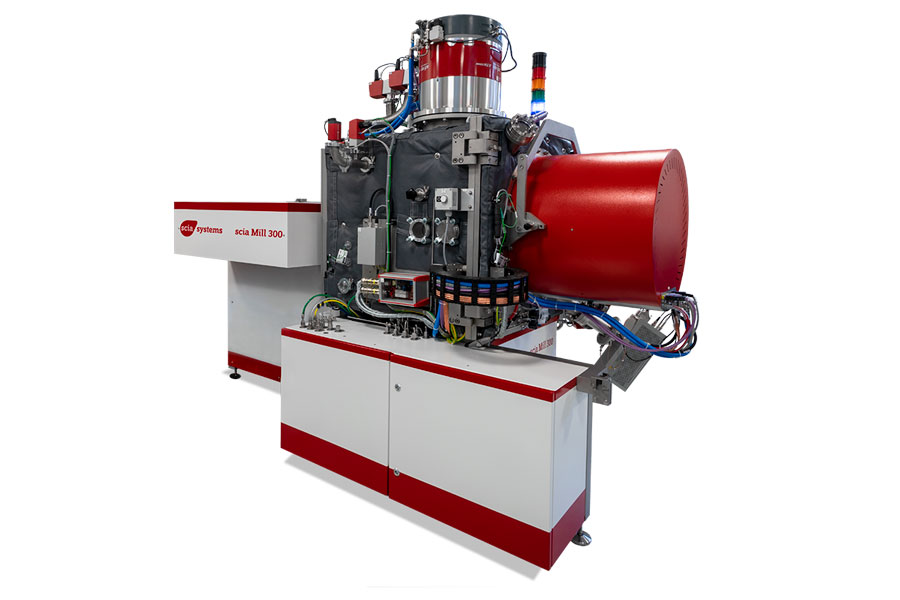
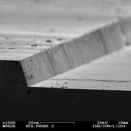
The scia Mill 150, 200, and 300 IBE systems are designed for etching and milling of substrates up to 150, 200, and 300mm diameter, respectively.
Etching modes:
- IBE with inert gases
- Reactive ion beam etching (RIBE) – usually F-based reactive gasses
- Chemically Assisted ion beam etching (CAIBE) – usually F- and Cl-based reactive gasses
The Mill 150 system is ideal for R&D applications and low volume production.
The Mill 200 and 300 systems can be implemented into a very compact cluster system, equipped with two Vacuum Cassette Elevators (VCE) and SEMS/GEM interface for high volume manufacturing.
Principle:
IBE (Inert gas in source, i.e. Ar, Kr, Xe)
RIBE (Reactive IBE, reactive gas in source)
CAIBE (Chemically Assisted IBE, reactive gas in gas ring)
Features and Benefits:
- Excellent uniformity without shaper
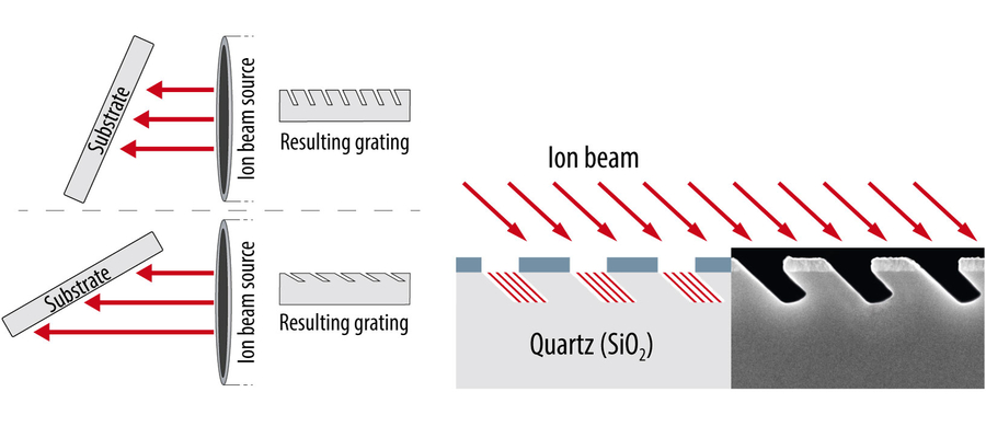
- Tiltable and rotatable substrate holder
- Ability to enhance selectivity and rate with reactive gasses
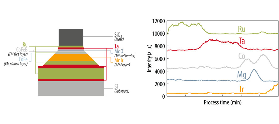
- Precise process control with SIMS or OES end point detection
- Helium backside contact cooling with water
- Allows for processing with photoresist with adequate wafer cooling
- Carrier concept enabling variable substrate sizes
Applications:
- Structuring of magnetic memory (MRAM) and sensors (IR, GMR, TMR)
- Milling of metals in MEMS production (Au, Pt, Ru, Ta, …)
- Milling of multilayers from diversified metal and dielectric materials
- RIBE or CAIBE of compound semiconductors (GaAs, GaN, InP, …)
- Production of 3D optoelectronic microstructures
- Ion beam smoothing for reduction of microroughness
- Pattern transfer for optical gratings
Technical Specifications:
| Mill 150 | Mill 200 | Mill 300 | |
|---|---|---|---|
| Substrate size | up to 150mm | up to 200mm | up to 300mm |
| Substrate rotation | 5-20 rpm | 5-20 rpm | 1-20 rpm |
| Substrate Tilt | 0° to 165°, in 0.1° steps | 0° to 170°, in 0.1° steps | 0° to 170°, in 0.1° steps |
| Substrate holder | Water-cooled, helium backside cooling contact | Water-cooled, helium backside cooling contact | Water-cooled, helium backside cooling contact |
| Ion beam source | 218mm circular microwave ECR source (MW218-e) | 350mm circular RF source (RF350-e) | 450mm circular RF source (RF450-e) |
| Neutralizer | Triple plasma bridge neutralizer (N-3DC) | RF plasma bridge neutralizer (N-RF) | RF plasma bridge neutralizer (N-RF) |
| Typical removal rate | SiO2: 30nm/min | SiO2: 20 nm/min (inert), 40-60 nm/min (reactive) Cu: 60 nm/min Pt: 35 nm/min W: 18 nm/min | SiO2: 20 nm/min (inert), 40-60 nm/min (reactive) Cu: 60 nm/min Pt: 35 nm/min W: 18 nm/min |
| Uniformity variation | ≤ 2 % (σ/mean) | ≤ 1 % (σ/mean) | ≤ 2 % (σ/mean) |
| Wafer throughput | NA | 12 Wafers/hr (100nm SiO2 removal on 200mm wafer) | 12 Wafers/hr (100nm SiO2 removal on 200mm wafer) |
| Base pressure | < 5 x 10⁻⁷ mbar | < 5 x 10⁻⁷ mbar | < 5 x 10⁻⁷ mbar |
| System dimension (W x D x H) | 1.70 m x 1.70 m x 1.70 m (without electrical rack) | 3.20 m x 2.50 m x 2.50 m 3 process chambers and cassette handler (without electrical racks and pumps) | 2.70 m x 1.50 m x 2.00 m Single chamber with single substrate load lock (without electrical racks and pumps) |
| Configurations | Single chamber Optional: single substrate load lock | Single chamber Optional: single substrate load lock or cassette handler Optional: Cluster system with up to 3 process chambers and cassette handler | Single chamber Optional: single substrate load lock or cassette handler Optional: Cluster system with up to 3 process chambers and cassette handler |
| End point detection | Option: none, OES, or SIMS | Optional: none, OES, or SIMS | Optional: none, OES, or SIMS |
| Software interfaces | SECS II / GEM, OPC | SECS II / GEM, OPC | SECS II / GEM, OPC |

